How Do You Convert Analog Dial Rone to Digital and Back Again
Dorsum in the 24-hour interval where the microprocessor was our standard edifice block, we tended to concentrate on computation and processing of data and not so much on I/O. Simply put there were a lot of things we had to become working just so we could and then read the state of an I/O port or a counter.
Nowadays the microcontroller has taken care of most of the system level needs with the luxury of built in RAM retentiveness and the power to upload our lawmaking. That leaves us able to concentrate on the major role of a microcontroller: to interpret something about the environs, make decisions, and oftentimes output the upshot to energize a motor, LED, or some other twiddly $.25.
Often the usefulness of a small microcontroller projection depends on being able to interpret external signals in the class of voltage or less often, electric current. For example the output of a photocell, or a temperature sensor may utilise an analog voltage to indicate brightness or the temperature. Enter the Analog to Digital Converter (ADC) with the ability to convert an external bespeak to a processor readable value.
ADC's
Converting analog to a digital format involves tradeoffs: how often you need to be updated every bit to the signal (sample rate), how much you need to know (resolution), and the cost (how much you accept in your pocket). High resolution and high speed tends have higher toll.
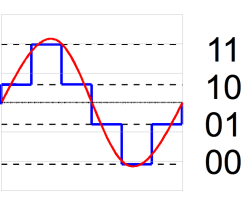
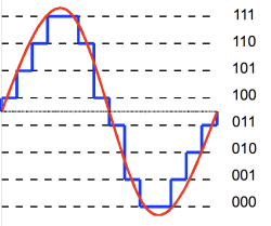
The human action of converting an analog value to a digital representation is somewhat mistake prone, and the tradeoffs deal with but how much error we can tolerate. Looking at the two diagrams below we come across a 3 flake digital representation of a sine moving ridge. The expanse between the blue digital "steps" and the red line indicates an amount of distortion of the original signal. Using more steps, or digital values and bits, we tin can reduce the baloney and our digital copy gets closer to faithfully representing the true signal.
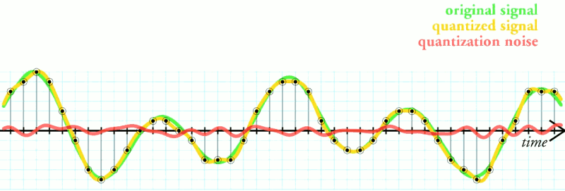
Also important is the sampling rate, or how oftentimes nosotros convert the analog signal to its digital counterpart. Simply as too few voltage "steps" (resolution) results in distortion, likewise few steps in time (sample charge per unit) too results in baloney. In this diagram the distance between the green and yellow lines represents time-based distortion as shown in red.
Types of ADC's
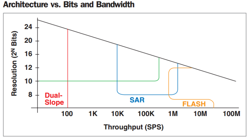
Looking at the chart below we see four of the most common ADC technologies and their capabilities. I could probably spend an entire video mail service talking about Delta Sigma as it combined digital and analog processing, here I will concentrate the other three: Flash, Successive Approximation and Dual-Slope.
Wink Blazon Converter
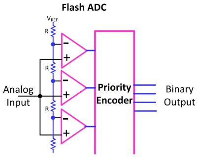 The Flash converter is the fastest, hence the name, but with some inherent limits to resolution and not without some cost involved. A flash converter is a drove of loftier speed comparators each with a slightly unlike voltage reference that they are comparison the signal to.
For 8 $.25 of resolution, a total of 256 comparators are needed forth with the supporting number of semi-precision resistors. Likewise a 10 bit converter needs 1024 comparators and herein lies the reason why flash converters, every bit high speed equally they are, are somewhat limited in resolution due to the problems with scaling equally the number of bits increase.
Too shown is a discreet signal to binary encoder known as a priority encoder. This logic creates a binary value representing the highest comparator active (think of information technology as the opposite of a decoder such every bit those used to create eight chip selects from 3 accost lines).
Successive Approximation Annals (SAR)
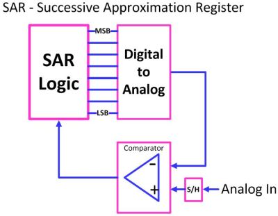 SAR utilizes a congenital-in Digital to Analog Converter (DAC), the reverse of an ADC, and compares the input point to the output of the DAC and makes adjustments until it closely approximates the input signal.
The SAR starts by first taking the MSB of the DAC value and setting it, representing 1/2 of full range, and so testing whether the input is greater or less than that value. The SAR then sets the scrap if information technology was greater, and so tests the side by side bit representing one/4 of the total. The SAR walks the bit on down testing for i/8, one/sixteen, 1/32 on down to the LSB, all the while setting a bit for when the input was greater.
This series of approximations gets more accurate every bit more bits are tested, effectively hunting down the best approximation for the voltage it is testing against. I evidence some examples using a spreadsheet to represent an eight bit SAR.
 First D7 is tested and if D7 is greater than the input (represented by red crosshatch) a zero is recorded, otherwise a ane is stored and D6 is tested (while remembering the state of D7). The conversion uses 1 cycle for each bit, so the SAR conversion shown takes 8 cycles each fourth dimension (vs. a unmarried acquisition time for wink).
I walk through this in the video but if you want a chance to work through this easily-on yous can download the SAR Adding Spreadsheet.
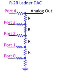
I have built an SAR system using an FPGA to provide the control logic, our R-2R Ladder that we built in the DDS video, and a simple comparator. Ever run across a microcontroller with a 1-chip comparator and wonder why information technology'south at that place? Hither is ane reason; you can brand an SAR with a handful or resistors on I/O ports and a 1-fleck comparator.
Sample and Hold
As stated, an viii bit SAR takes 8 cycles to complete an acquisition. During this fourth dimension it is important that the voltage non change value as the series of approximations take place.
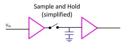
Enter the Sample and Concur (S/H) circuit. In its simplest class it captures the indicate value in the course of a accuse on a capacitor and then is isolated by a switch that disconnects the input. South/H circuits are available equally integrated circuits that likewise exercise things like minimize the belch of the voltage on the capacitor, known equally droop, and to make sure that the switch affected the indicate a minimal amount.
Dual Gradient
Dual Gradient conversion is named after the fact that it integrates the input bespeak for a known period of time, which results in an accumulated charge equal to the input signal, while providing some low pass filtering in the process. The charge is then integrated off by applying a known reference voltage in the opposite polarity and counting clock pulses until the signal returns to zilch. Between each of these measurement cycles is an auto-zero stage which helps remove effects like globe-trotting baseline.
Dual-Slope is used in instances where higher resolution is needed and conversion fourth dimension isn't as critical. As Dual-Slope can also be low ability consumption information technology is often found in handheld devices like Volt-Ohm Meters or in the example I bear witness at the cease, precision digital weighing instrumentation.
The output of Dual-Slope is ultimately a string of clock pulses though they may exist internally converted to a binary value such equally in the case of the TC7109 IC I show above. In cases where output is a cord of pulses that need to be counted, a microcontroller can count them using dedicated counting circuitry or counting overflows of an external split down counter where each overflow represents a known quantity of pulses. A trick for using an external counter to exercise scaling and yet become the do good of the full resolution is to then manually pulse the counter until the very last overflow is detected. The number of manual pulses it took is used to determine how many were left in the counter afterwards the conquering phase.
Putting it Together
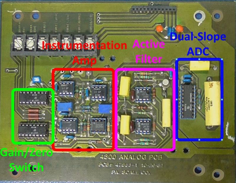
Below you lot can run into a precision analog department I did back in 1982. Included in the design is a Dual-Slope ADC, an Instrumentation Amplifier with Cipher and Proceeds correction (similar to Chopper-Stabilized or Goose egg-Migrate amps) and active filters, all of which we accept covered in Hackaday videos. The design is nonetheless viable all the same it is now possible to replace the instrumentation amplifier with a small-scale dedicated chip and the dual-slope converters run faster with smaller capacitors, which takes some of the requirements off of the capacitor to not exhibit quite as low of leakage or dielectric absorption.
Conclusion
Understanding how an ADC works can be useful in understanding the results returned, or whether a dissimilar technology should ultimately be used. These days with SPI and IiiC interfaces available on a wide array of ADC's they can exist connected to almost any processor compages with minimal demand to consider information autobus architecture and timing.
Source: https://hackaday.com/2016/05/05/analog-to-digital-conversion/
0 Response to "How Do You Convert Analog Dial Rone to Digital and Back Again"
Postar um comentário